

650V Super-junction Power Mosfet
Super-junction Power Mosfet
A super-junction (SJ) power MOSFET is a type of MOSFET that uses a special charge-compensation structure of alternating N-type and P-type semiconductor regions to achieve lower on-resistance, while blocking high voltages. This structure allows for more efficient power conversion by improving overall efficiency, reducing losses, and enabling smaller device sizes in applications like power supplies, LED lighting, and electric vehicle chargers.
Structure and operation
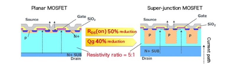
Super-junction structure: Instead of a simple planar structure, SJ MOSFETs use a drift region with columns of alternating P-type and N-type doping.
Charge compensation: When a voltage is applied, the depletion layers of these columns expand both vertically and horizontally. The arrangement of P and N columns allows the depletion layers to merge into a single layer that extends across the entire drift region, which significantly increases the voltage the device can withstand for a given resistivity.
Reduced resistance: By using this super-junction structure, manufacturers can reduce the silicon’s resistivity, which leads to a much lower on-resistance compared to conventional MOSFETs at the same voltage rating.
Advantages
Lower on-resistance : Significantly lower resistance leads to reduced conduction losses and heat buildup.
Improved efficiency: Lower losses result in higher overall power efficiency, which is critical for applications requiring high efficiency.
Smaller size: Higher efficiency and power density can lead to smaller package sizes for the same performance.
High voltage capability: The super-junction structure enables the devices to block high voltages (e.g., 250 V to 650 V) while maintaining low on-resistance.
Topdiode Super-junction Power Mosfet TAPA65R380KM can perfectly replace Infineon IPD60R385CPATMA1:
Features
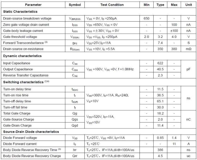
⚫650V,11A
RDS(ON)<380mΩ@VGS=10V TYP:350mΩ
⚫ advanced super junction technology
⚫ extremely low on resistance


ABSOLUTE MAXIMUM RATINGS (Ta=25℃ unless otherwise noted)

MOSFET ELECTRICAL CHARACTERISTICS(Ta=25℃ unless otherwise noted)
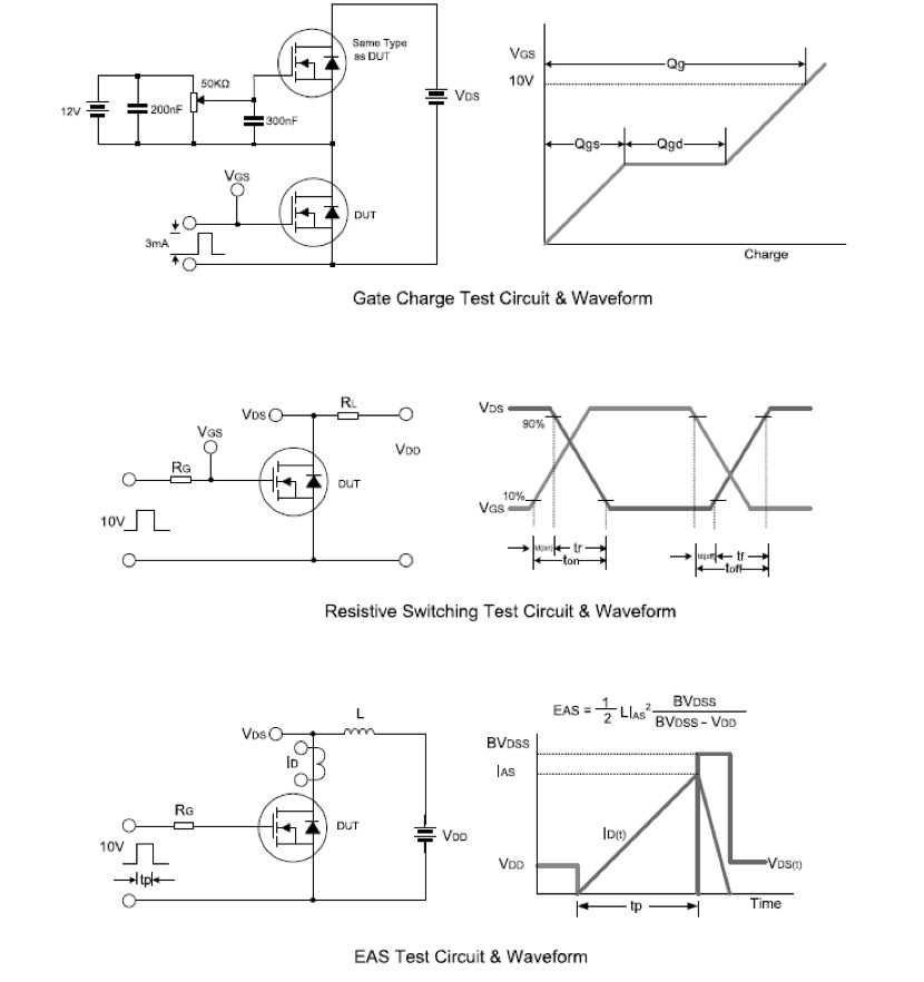
Test Circuit
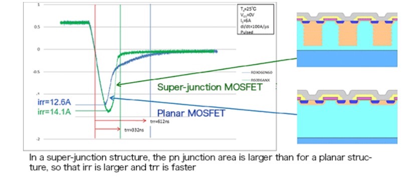
Conclusions
The superjunction structure is a major development in high-voltage MOSFET technology and offers significant benefits. RDS(on), gate capacitances, and output charge are all simultaneously reduced, along with die size. To make the best use of these fast and efficient devices, designers have to pay greater attention to their system design, particularly towards reducing PCB parasitics. Superjunction MOSFETs have much lower gate charges and can be driven with low-current gate drivers. Their output capacitances, while highly non-linear, offer lower stored energy Eoss and related output losses. Topdiode superjunction devices are available in different packages, voltage ratings, and body diode characteristics to suit a wide variety of applications.