

Comparative Analysis of NMOS and PMOS Technologies
What is NMOS?
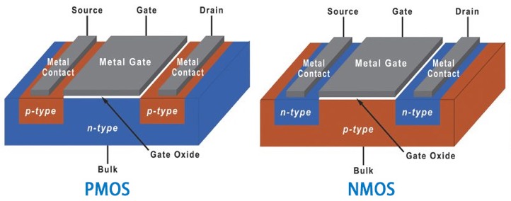
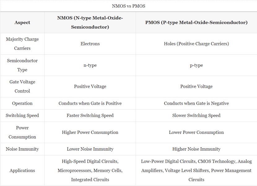
NMOS (N-type Metal Oxide Semiconductor) is a type of Metal-Oxide-Semiconductor Field-Effect Transistor (MOSFET) where the majority carriers are electrons. In NMOS transistors, the source and drain are formed by N-type regions diffused into a P-type substrate. When a positive voltage is applied to the gate relative to the source, an electric field attracts electrons toward the SiO₂ interface, forming a conductive inversion channel that allows current to flow between the source and drain.
What is PMOS?
PMOS (P-type Metal Oxide Semiconductor) is another type of MOSFET where the majority carriers are holes. PMOS transistors are built on an N-type substrate, with the source and drain formed by P-type regions. When a negative voltage is applied to the gate relative to the source, the electric field repels electrons and accumulates holes at the SiO₂ interface, thereby creating a conductive channel for current flow.
Structural Differences
NMOS Structure
✦ Substrate: P-type semiconductor
✦ Source/Drain: N-type regions
✦ Gate: Separated from the substrate by a thin SiO₂ layer with a conductive gate electrode (typically polysilicon or metal)
✦ Operation: A positive gate voltage attracts electrons to form an inversion channel enabling conduction
PMOS Structure
✦ Substrate: N-type semiconductor
✦ Source/Drain: P-type regions
✦ Gate: Similar to NMOS, consisting of an SiO₂ insulation layer and a conductive gate electrode
✦ Operation: A negative gate voltage repels electrons and accumulates holes to form a conductive channel
✦ In both cases, the gate voltage effectively controls the conductivity of the channel, allowing MOSFETs to function as switches or amplifiers.
Advantages of NMOS
- Higher speed: Due to higher electron mobility, NMOS transistors switch faster than PMOS.
- Higher integration density: NMOS devices can be made smaller under the same process conditions, enabling denser circuits.
Limitations of NMOS
- Higher power consumption: NMOS typically consumes more power in the “on” state.
- Lower noise margin: More sensitive to noise compared to PMOS circuits.
- Manufacturing cost: Despite smaller device sizes, overall cost may depend on process complexity.
Advantages of PMOS
- Lower power consumption: Consumes less power when conducting, making it suitable for low-power applications.
- Better noise tolerance: Provides higher noise margins, enhancing reliability in some designs.
- Mature process: PMOS technology was simpler and widely adopted before NMOS became dominant.
Limitations of PMOS
- Slower switching: Hole mobility is lower than electron mobility, resulting in slower operation.
- Lower integration density: PMOS devices cannot be scaled as small as NMOS, limiting circuit density.
Performance Comparison
Applications
‣NMOS Applications
‣High-speed digital logic circuits
‣Microprocessors and high-performance computing
‣Dynamic Random Access Memory (DRAM) cells
PMOS Applications
‣Low-power or battery-operated devices
‣Pull-up devices in CMOS logic gates
‣Analog switches and multiplexers
NMOS and PMOS technologies each have distinct advantages and trade-offs. NMOS offers higher speed and density, making it well-suited for high-performance and cost-sensitive applications. PMOS, with its lower leakage current and stronger noise tolerance, is more suitable for low-power and high-voltage environments. With the evolution of CMOS technology, the complementary use of NMOS and PMOS has become the foundation of modern integrated circuit design, leveraging the strengths of both device types.
FAQ
Why is NMOS much faster than PMOS?
The speed of a transistor depends on the mobility of the charge carriers flowing through it. In an NMOS transistor, the carriers are electrons, which have higher mobility compared to holes, the carriers in PMOS transistors. This means that under the same applied voltage, electrons move faster, resulting in a higher switching speed for NMOS devices.
Is PMOS larger than NMOS?
Yes. Since hole mobility is lower than electron mobility, PMOS devices generally need to be larger in size to provide the same drive current capability as NMOS devices.
Why is NMOS better than PMOS?
NMOS devices switch faster due to the higher electron mobility, and they can be made smaller than equivalent PMOS devices, allowing higher circuit density.
Why is CMOS better than NMOS or PMOS alone?
CMOS technology combines the best characteristics of both: the fast switching speed of NMOS and the low static power consumption of PMOS. This makes CMOS circuits more power-efficient, especially for battery-powered and portable applications.