

Selection of Transient Voltage Suppression (TVS) Diodes in Circuit Design
The Transient Voltage Suppression (TVS) diode is an overvoltage protection device with bidirectional voltage regulation and negative resistance characteristics, similar to varistors. It is widely used in various AC and DC power circuits to suppress instantaneous overvoltages. When a surge pulse voltage occurs in the protected circuit, the bidirectional breakdown diode rapidly undergoes Zener breakdown, transitioning from a high-impedance state to a low-impedance state, thereby shunting and clamping the surge voltage to protect circuit components from damage caused by transient voltage spikes.
Key Features
- Extremely fast response time (picosecond level)
- Surge withstand capability is inferior to gas discharge tubes and varistors
- Pulse power handling: 400W to 30KW for 10/1000μs waveform
- Peak pulse current range: 0.52A to 544A
- Breakdown voltage options: 6.8V to 550V series for various circuit voltage requirements
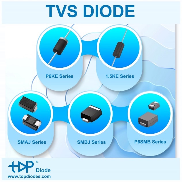
Package Types
Surface Mount
- SMAJ (400W)
- SMBJ (600W)
- SMCJ (1.5kW)
- SMDJ (3kW) series
Axial Lead
- P4KE (400W)
- SA (500W)
- P6KE (600W)
- 5KE (1.5kW)
- 3KP (3kW)
- 5KP (5kW)
- 15KPA (15kW)
- 20KPA (20kW)
- 30KPA (30kW) series
- Low capacitance SAC series (500W, 50pF)
- BZW04 (400W) series glass-passivated junction TVS diodes
Key Parameters
Maximum Reverse Leakage Current (IR) and Stand-off Voltage (VR=VRWM)
- VR is the maximum DC working voltage of the TVS diode
- When voltage across the TVS is below VR, it remains in the off state with maximum leakage current IR
Breakdown Voltage (VBR) and Test Current (IT)
- VBR is the minimum avalanche voltage of the TVS
- When reverse voltage reaches VBR, the TVS becomes a low-impedance path
- Typically measured at IT = 1mA current flow
Maximum Clamping Voltage (VC) and Peak Pulse Current (IPP)
- VC is the maximum voltage across the TVS during IPP flow
- VC and IPP represent the surge suppression capability
- Clamping factor (VC/VBR ratio) is typically ~1.3
- Lower clamping factor indicates better transient suppression
- TVS diodes have significantly lower clamping factors than MOVs, making them superior for protection
Junction Capacitance (C)
- Determined by the TVS avalanche junction area
- Measured at 1MHz frequency
- Higher C correlates with greater current handling capability
- Excessive C causes signal attenuation
- Critical parameter for data interface circuits
Peak Pulse Power Dissipation (PPPM)
- Maximum pulse power handling capability (PPPM = VC × IPP)
- Higher PPPM at given VC indicates greater surge current capability
- Lower VC at given PPPM indicates greater surge current capability
- PPPM also depends on pulse waveform, duration, and ambient temperature
Clamping Response Time (TC)
- Time from off-state to reaching VBR
- <1×10⁻¹²s for unipolar TVS devices
- <10ns for bipolar TVS devices
Working Principle
TVS diodes (Zener-type) are primarily used for ESD protection, absorbing electrostatic discharges and short voltage pulses from external interfaces and terminals. In normal operation, they present high impedance to the protected circuit. When transient voltage exceeds the breakdown voltage, the TVS diode provides a low-impedance path, diverting surge current through itself while limiting the protected component’s voltage to the clamping level. After the overvoltage condition ends, the TVS diode returns to its high-impedance state.
Topdiode supply wide range of TVS diodes, welcome send RFQ: