

TAP2302B: The Superior, Drop-in Replacement for ON Semi FDN327N P-Channel MOSFET
In the fast-paced world of electronics design and manufacturing, component obsolescence, long lead times, and supply chain disruptions are constant challenges. When a trusted part like the ON Semiconductor FDN327N becomes difficult to source, finding a reliable, high-performance alternative is not just a preference—it’s a necessity for business continuity.
Meet the TAP2302B, a robust P-Channel Enhancement Mode MOSFET from a trusted Chinese manufacturer. Engineered for excellence, the TAP2302B is designed as a direct, drop-in replacement for the FDN327N, offering not just parity but, in many key parameters, superior performance. This article delves deep into the technical specifications, performance benefits, and application suitability of the TAP2302B, making the case for why it should be your go-to choice.
Understanding the Application: Why the FDN327N is Popular
First, let’s understand the role of the FDN327N. This -30V, -3.1A P-Channel MOSFET in a compact SC-70-3/SOT-323 package is a workhorse in numerous low-voltage, space-constrained applications. Its primary functions include:
- Load Switching: Power management in battery-operated devices (phones, tablets, portable gadgets).
- Power Distribution: Switching power rails on PCBs.
- Logic Level Shifting: Interface between controllers and power circuits.
- Motor Control: Driving small DC motors in consumer electronics.
The key requirements for a MOSFET in these roles are low gate drive voltage, low on-resistance (RDS(ON)), high efficiency, and a small footprint. Any replacement must meet or exceed these criteria.
TAP2302B vs. FDN327N: A Head-to-Head Technical Comparison
Table1.TAP2302B
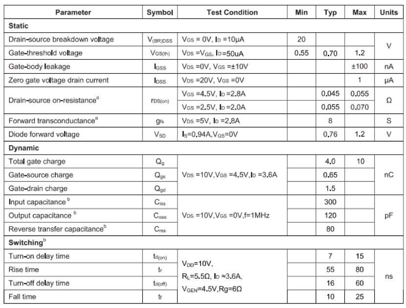
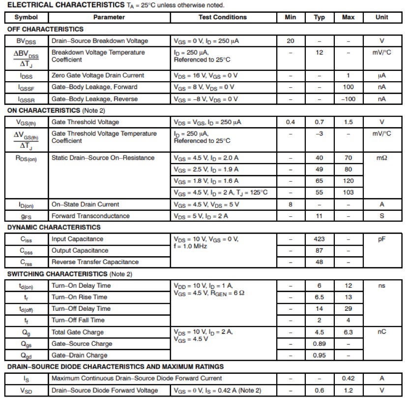
Table2.FDN327N
Key Advantages of Choosing TAP2302B
As the comparison shows, the TAP2302B doesn’t just match the FDN327N—it outperforms it in critical areas.
Lower On-Resistance (RDS(ON)) for Higher Efficiency
The most significant figure of merit for a MOSFET in switching applications is its on-resistance.The TAP2302B boasts a lower RDS(ON) at both standard (-10V) and logic-level (-4.5V) gate drives.
- What this means for your design: Lower RDS(ON) translates directly to reduced conduction losses (I²R). This means the MOSFET dissipates less power as heat, leading to:
- Higher overall system efficiency, extending battery life in portable devices.
- Cooler operation, enhancing long-term reliability and thermal management.
- The ability to handle the same current with less voltage drop.
Higher Continuous Drain Current
With a maximum continuous drain current of-3.5A compared to the FDN327N’s -3.1A, the TAP2302B offers a greater margin of safety and capacity.
- What this means for your design: This higher current rating provides extra headroom for surge currents and varying load conditions. It makes the TAP2302B a more robust solution, potentially allowing it to be used in applications that are slightly more demanding than the original FDN327N’s specification.
Drop-in Replacement with Guaranteed Compatibility
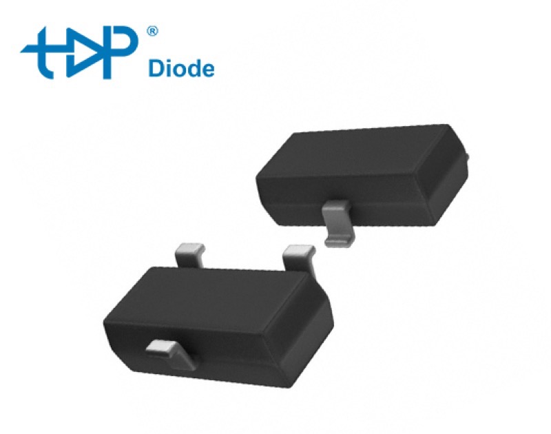
We understand that redesigning a PCB is costly and time-consuming.The TAP2302B is packaged in the industry-standard SC-70-3/SOT-323. Its pinout (Gate, Source, Drain) is identical to the FDN327N. You can confidently replace the FDN327N with the TAP2302B on your existing board without any layout modifications.
Superior Quality and Reliability from a Trusted Source
As a dedicated Chinese manufacturer of electronic components,we have built our reputation on quality and reliability. The TAP2302B is manufactured in state-of-the-art facilities with strict process control, ensuring:
- Consistent performance across high-volume production runs.
- High reliability and long operational lifespan.
- Compliance with international quality standards.
Application Circuits: Where to Use the TAP2302B
The TAP2302B excels in the same applications as the FDN327N. Here are two common circuit examples:
Load Switch Circuit:
In this configuration,a microcontroller GPIO pin controls the power to a load (e.g., a sensor module). The P-Channel MOSFET is placed on the high side.
- The source is connected to the power supply (e.g., 3.3V or 5V).
- The drain is connected to the load (VOUT).
- The gate is controlled by the microcontroller via a small N-Channel MOSFET or a resistor for direct logic-level control.
The low RDS(ON) of the TAP2302B ensures minimal voltage drop from the supply to the load, guaranteeing the load receives the full required voltage.
Reverse Polarity Protection Circuit:
A P-Channel MOSFET can be used for simple and efficient reverse polarity protection without the power loss of a diode.
- The MOSFET is placed in the positive rail.
- The body diode is oriented to allow current flow when polarity is correct.
- Upon correct connection, the gate-source voltage becomes negative, turning the MOSFET fully on and shorting the body diode, thus minimizing voltage drop.
The TAP2302B’s -30V drain-source voltage and robust construction make it ideal for this protective role.
Conclusion: Make the Smart Switch to TAP2302B
In the search for an FDN327N alternative, the TAP2302B stands out not as a mere substitute, but as a strategic upgrade. It offers lower power loss, higher current handling, and cooler operation while maintaining perfect physical and electrical compatibility.
By choosing the TAP2302B, you are not just solving a supply chain problem; you are enhancing the performance and reliability of your product. You gain a dependable partner committed to delivering high-quality components without compromise.
Learn more by visiting our website!