

Topdiode TPA06P5K4L cross for onsemi NDS0605
The Topdiode TPA06P5K4L is a P-channel enhancement-mode Metal-Oxide-Semiconductor Field-Effect Transistor (MOSFET) designed for low-power switching applications. As a compact and efficient power device, it is widely used in modern electronic circuits where space efficiency, fast switching, and low power consumption are critical design requirements.
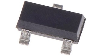
Unlike traditional mechanical relays, the TPA06P5K4L offers significantly faster switching speed, higher efficiency, and longer operational life, while occupying minimal PCB area. Housed in a SOT-23 surface-mount package, the device features three terminals, each serving a specific electrical function.
Key Features
Pin Configuration and Functions
The TPA06P5K4L adopts a standard SOT-23 pin assignment:
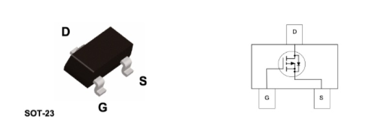
Pin 1: Gate (G)
The gate is the control terminal of the MOSFET. By applying an appropriate voltage to the gate relative to the source, the conduction state of the device can be controlled. As a P-channel MOSFET, the TPA06P5K4L turns on when a negative gate-to-source voltage (VGS) is applied.
Pin 2: Drain (D)
The drain is the current output terminal. In practical applications, it is typically connected to the load being controlled.
Pin 3: Source (S)
The source is the current input terminal and is usually connected to the power supply or a reference voltage.
Note: While pin assignments may vary among different SOT-23 devices, the TPA06P5K4L follows the standard configuration: gate on the left, drain in the center, and source on the right.
Applications of TPA06P5K4L
1. Power Management
The TPA06P5K4L is commonly used in DC-DC converters and load-switch circuits, where it efficiently controls current flow to maintain stable voltage output. Its low on-resistance (RDS(on)) minimizes conduction losses and heat generation, improving overall power efficiency and system reliability.
2. Portable and Battery-Powered Devices
Compact, power-sensitive products such as smartwatches, wireless earbuds, power banks, and smartphones benefit from the TPA06P5K4L’s small SOT-23 footprint and high efficiency. These characteristics help conserve PCB space and extend battery life, enabling longer device operation.
3. Industrial Control
In automation and industrial control systems, the TPA06P5K4L is often used to drive small motors, relays, or LED indicators. Its fast switching performance ensures quick response to control signals, improving system accuracy and operational reliability.
4. New Energy and Internet of Things (IoT)
Thanks to its low power consumption and high efficiency, the TPA06P5K4L is well suited for low-power control and switching circuits. It is widely used in battery-powered sensor nodes and smart home devices, meeting the demands of modern energy-efficient designs.
TPA06P5K4L Selection Guide
Before integrating the TPA06P5K4L into your design, it is essential to evaluate its electrical characteristics against your application requirements.
1. Voltage and Current Ratings
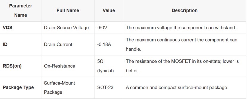
Ensure that the drain-to-source voltage (VDS) and continuous drain current (ID) meet the load conditions. The TPA06P5K4L is rated at –60 V and –0.18 A, making it ideal for low-current switching applications. Adequate design margin should be reserved to handle transient voltage spikes and inrush currents.
2. Power Dissipation and Thermal Management
The device’s low RDS(on) reduces conduction losses; however, power dissipation must still be carefully managed. The maximum power dissipation is 0.5 W. Due to the limited thermal capability of the SOT-23 package, it is recommended to provide sufficient copper area on the PCB, especially under the drain pin, to enhance heat dissipation and ensure long-term stability.
3. Gate Drive Voltage
As a P-channel MOSFET, the TPA06P5K4L requires a negative VGS to turn on fully. Designers should ensure that the driving circuit—such as a microcontroller or dedicated driver IC—can provide adequate gate voltage swing to achieve optimal switching performance and minimum on-resistance.
4. Package Considerations
The SOT-23 package is well suited for high-density PCB layouts and space-constrained designs. However, precise soldering and proper PCB layout are essential to maintain electrical and thermal performance.
Important Design Note
In high-frequency switching applications, additional dynamic losses may occur due to frequent switching transitions. If total power dissipation exceeds the maximum rating, the device may overheat or fail. Proper thermal design, accurate power calculations, and conservative operating margins are crucial for reliable operation.
Frequently Asked Questions (FAQ)
Q1: Which devices can replace the TPA06P5K4L?
The TPA06P5K4L can serve as a replacement for devices such as Fairchild NDS0610, Vishay Si2303DS, and NXP BSS84, provided that key parameters—including VDS, ID, RDS(on), and package type—are carefully compared to ensure compatibility.
Q2: How can I test the TPA06P5K4L?
Basic functionality can be verified using a multimeter.
Diode Mode Test:
Set the multimeter to diode mode. For a P-channel MOSFET, the body diode conducts from source to drain. Place the red probe on the source and the black probe on the drain. A forward voltage drop of approximately 0.5–0.7 V indicates normal operation.
Switching Test:
Set the multimeter to resistance mode. With probes across source and drain, the device should show high resistance. Applying a negative charge between gate and source should cause the resistance to drop significantly, indicating conduction.
Q3: What voltage and current ranges is the TPA06P5K4L suitable for?
The TPA06P5K4L is designed for medium-voltage, low-current applications. It is suitable for 12 V, 24 V, and 48 V DC systems, and for driving small loads such as relay coils, indicator LEDs, and low-power motors. It is not intended for high-power load switching.
Q4: Common Issues and Solutions
Overheating: Check for excessive current or high switching frequency; improve PCB heat dissipation.
Incomplete switching: Ensure sufficient negative gate-to-source voltage.
Device damage: Protect against ESD, voltage spikes, and overcurrent using proper handling and protective circuitry.