

Types of TVS Diodes & TVS Diode Selection Parameters
1. Types of TVS Diodes
1.1 Unidirectional TVS Diodes
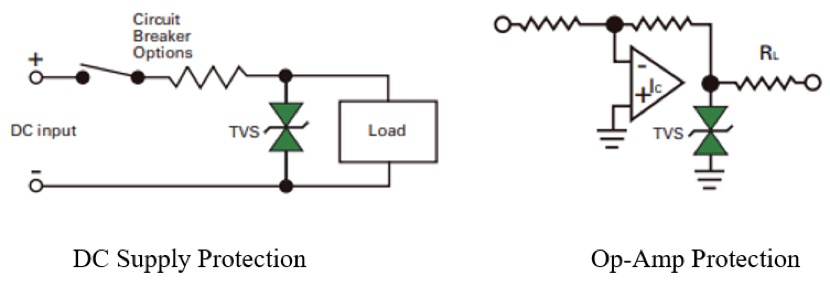
Unidirectional TVS diodes are primarily used in direct current (DC) circuits to protect against transient voltages in either the positive or negative direction (depending on the installation direction). They provide standard diode forward conduction characteristics (typically around 0.7V forward voltage drop) in one direction and avalanche breakdown protection in the opposite direction.
Key characteristics include:
- Suitable for unipolar signal lines and DC power lines
- Lower clamping voltage compared to equivalent bidirectional TVS
- Typical applications include DC power lines, MOSFET gate protection, etc.
“When selecting a unidirectional TVS diode, ensure its reverse working voltage is slightly higher than the maximum operating voltage of the system, which ensures it won’t conduct under normal operating conditions.” — Circuit Protection Design Manual
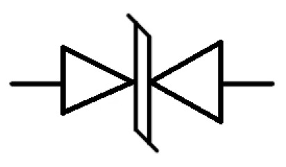
1.2 Bidirectional TVS Diodes
Bidirectional TVS diodes are essentially two unidirectional TVS connected back-to-back in series, providing similar protection characteristics in both directions. They are particularly suitable for alternating current (AC) signal lines and data lines that require protection in both positive and negative directions.
The main applications of bidirectional TVS diodes include:
- AC signal and power lines
- Bipolar signals (such as audio signals)
- Data communication lines (such as RS-232, RS-485, CAN bus, etc.)
- I/O port protection
Compared to unidirectional TVS, bidirectional TVS typically have symmetrical breakdown voltages in both directions, making them particularly suitable for protecting AC signals and bipolar data lines.
1.3 TVS Diode Arrays
TVS diode arrays are devices that integrate multiple TVS diodes in a single package, designed specifically for protecting multi-line interfaces (such as USB, HDMI, Ethernet, etc.). They typically come in small packages suitable for space-constrained applications.
The main advantages of TVS arrays:
- Multi-channel protection, reducing PCB space usage
- Simplified design and layout
- More consistent protection characteristics
- Reduced overall wiring complexity and parasitic effects
Common TVS array packages include SOT-23-6/8, SOIC-8, QFN, and ultra-small DFN/CSP packages designed for portable electronic devices and high-density PCB designs.
1.4 Important Note
When selecting TVS arrays, consider the coupling effects between channels. High-quality TVS array designs should ensure that a transient event on one channel does not affect other channels through parasitic coupling.
2 TVS Diode Selection Parameters
2.1 Key Parameters
Selecting suitable TVS diodes requires consideration of multiple key parameters, which collectively determine the device’s protection capability and application range:
| Parameter | Symbol | Definition | Selection Consideration |
| Reverse Working Voltage | VRWM | Maximum reverse voltage that the device can continuously withstand | Should be greater than the system’s maximum operating voltage |
| Reverse Breakdown Voltage | VBR | Voltage at which the device begins to enter avalanche state | Typically 1.1~1.5 times VRWM |
| Clamping Voltage | VC | Maximum voltage at specific test current | Should be lower than the voltage tolerance of the protected component |
| Peak Pulse Current | IPP | Maximum transient current the device can withstand | Should be greater than the current of expected transient events |
| Peak Pulse Power | PPP | Maximum transient power the device can absorb | Depends on application scenario and expected threat level |
| Reverse Leakage Current | IR | Leakage current at VRWM | Should be low enough to not affect normal operation |
| Junction Capacitance | CJ | Parasitic capacitance of TVS diode | Low capacitance types should be selected for high-speed signal lines |
Professional Tip
For high-speed data lines (such as USB 3.0, HDMI, PCIe, etc.), selecting low-capacitance TVS diodes is crucial. Higher parasitic capacitance can lead to signal integrity issues and data transmission errors. Modern low-capacitance TVS diodes typically have capacitance values as low as 0.5pF.
2.2 Selection Guide
Selecting appropriate TVS diodes is key to ensuring effective protection. Here is a systematic selection process:
- Determine the system’s maximum operating voltage: Analyze the normal voltage range of the protected circuit, including possible fluctuations.
- Select reverse working voltage (VRWM): Should be slightly higher than the system’s maximum operating voltage, ensuring the TVS doesn’t conduct during normal operation.
- Determine the voltage tolerance of the protected device: This will determine the required upper limit of clamping voltage (VC).
- Evaluate transient threat types and levels: Determine the required protection level based on application environment (industrial, automotive, consumer electronics, etc.) and applicable standards (IEC 61000-4-2/4/5, etc.).
- Determine peak pulse current/power requirements: Should be based on worst-case transient event analysis.
- Consider signal bandwidth requirements: High-speed signals require low-capacitance TVS devices.
- Evaluate space limitations and heat dissipation conditions: Select appropriate packaging.
Reference selection criteria for different applications:
- Power line protection: Select VRWMslightly higher than maximum power supply voltage, consider higher power handling capability
- Data line protection: Prioritize low-capacitance models, ensure signal integrity
- Automotive electronics: Select TVS diodes that comply with AEC-Q101 certification, wide operating temperature range, and high energy handling capability
- Portable devices: Consider small package size and low leakage current characteristics
2.3 Package Types
TVS diode packages are diverse, ranging from power devices to miniature surface-mount packages. Selecting the appropriate package is crucial for meeting space, power, and heat dissipation requirements:
| Package Type | Size Characteristics | Power Handling Capability | Typical Applications |
| DO-214 (SMA, SMB, SMC) | Medium-sized SMD package | 400W – 5000W | Power lines, industrial interface protection |
| SOD-123/SOD-323 | Small SMD package | 150W – 500W | Medium to low power applications, space-constrained scenarios |
| SOT-23/SOT-363 | Small multi-pin package | 100W – 300W | Multi-channel protection, data lines |
| DFN/CSP | Ultra-small package | 50W – 200W | Mobile devices, wearable devices |
| QFN/SOIC | Multi-channel array package | Varies by number of channels | Multi-line interface protection (USB, HDMI, etc.) |
Important Note
When selecting a package, consider power dissipation capability simultaneously. For high-power applications, ensure the PCB design provides sufficient heat dissipation paths, such as increasing copper foil area, adding thermal vias, etc. Improper heat dissipation can significantly reduce the actual protection capability of TVS diodes.