


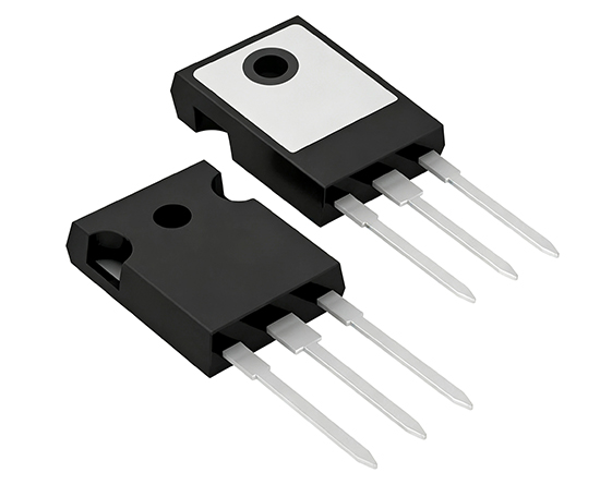
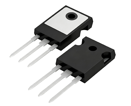
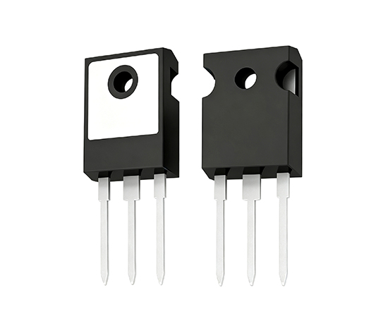
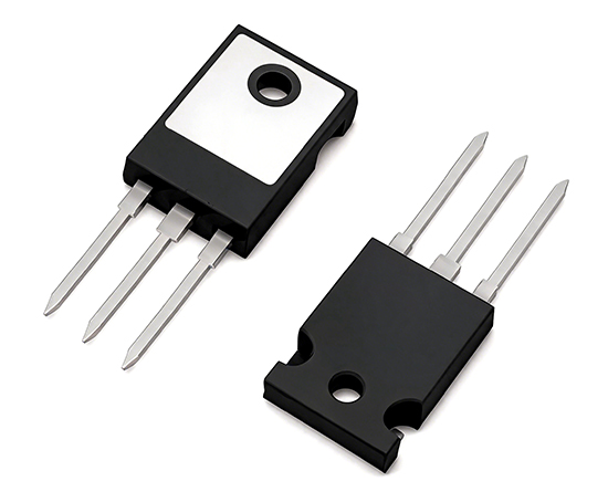
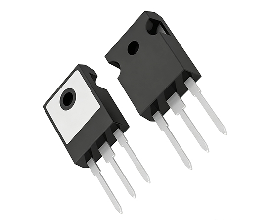
Topdiode MBR8040PT is a nice alternative offer for Vishay VS-80CPQ150-N3
- High efficiencty operation and Low power loss
- Low stored charge majority carrier conduction
- High forward surge capability
- Lead free in compliance with EU RoHS
- 2011/65/EU directive
- Green molding compound as per IEC61249 Std..(Halogen Free
Topdiode MBR8040PT is a nice alternative offer for Vishay VS-80CPQ150-N3
Topdiode MBR8040PT is a high-current Schottky rectifier designed for high-frequency and high-efficiency power conversion applications
Topdiode MBR8040PT is a nice alternative offer for Vishay VS-80CPQ150-N3
Schottky Barrier Rectifiers MBR8040PT -Topdiode DATA
- Tab
| RATINGS | SYMBOL | MBR8040PT | MBR8045PT | MBR8060PT | MBR80100PT | MBR80150PT | MBR80200PT | UNIT |
| Maximum repetitive reverse voltage | VRRM | 40 | 45 | 60 | 100 | 150 | 200 | V |
| Maximum RMS voltage | VRMS | 28 | 32 | 42 | 70 | 105 | 140 | V |
| Maximum DC blocking voltage | VDC | 40 | 45 | 60 | 100 | 150 | 200 | V |
| Maximum average per device forward current per diode |
IAV | 80 | A | |||||
| 40 | ||||||||
| Peak forward surge current, 8 .3ms single half sine-wave superimposed on rated load | IFSM | 500 | A | |||||
| Typical thermal resistance (Note 1) | Rθ-JC | 1.5 | °C/W | |||||
| Operating junction temperature range | TJ | -55 to +150 | -55 to +175 | °C | ||||
| Storage temperature range | TSTG | -55 to +175 | °C | |||||
| CHARACTERISTICS | SYMBOL | MBR8040PT | MBR8045PT | MBR8060PT | MBR80100PT | MBR80150PT | MBR80200PT | UNIT |
| Maximum forward voltage per leg IF=30A IF=40A | VF | 0.6 | 0.7 | 0.8 | 0.88 | V | ||
| 0.65 | 0.75 | 0.85 | 0.95 | |||||
| Maximum average reverse current at rated DC blocking voltage |
IR | 0.1 | 0.02 | 0.01 | mA | |||
| TJ=25°C TJ=100°C | 30 | 10 | 5 | |||||
Topdiode Hot Selling Products (6)
-
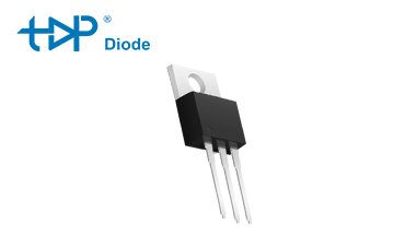
Topdiode Silicon-carbide (SiC) Schottky Barrier Diode, replace Infineon, On Semi, Littelfuse etc.
-
-
-
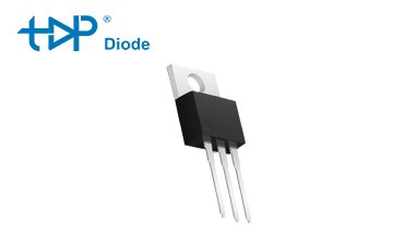
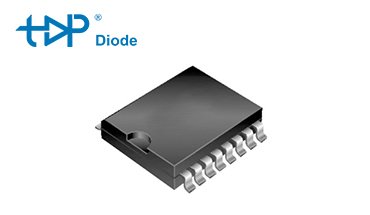
Topdiode Insulated Gate Bipolar Transistors (IGBT), replace Infineon, On semi, ST, AOS etc.
-
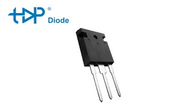
Topdiode Silicon-carbide (SiC) Power MOSFET, replace Infineon, On Semi, ROHM etc.
-
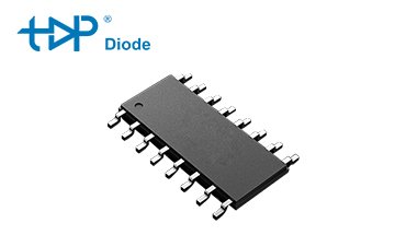
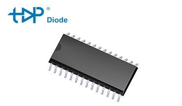
Topdiode Audio Amplifier Audio IC TPA2092 and TPA20957, replace Infineon IRS2092 and IRS20957S
SiC Schottky Barrier Diode Datasheet
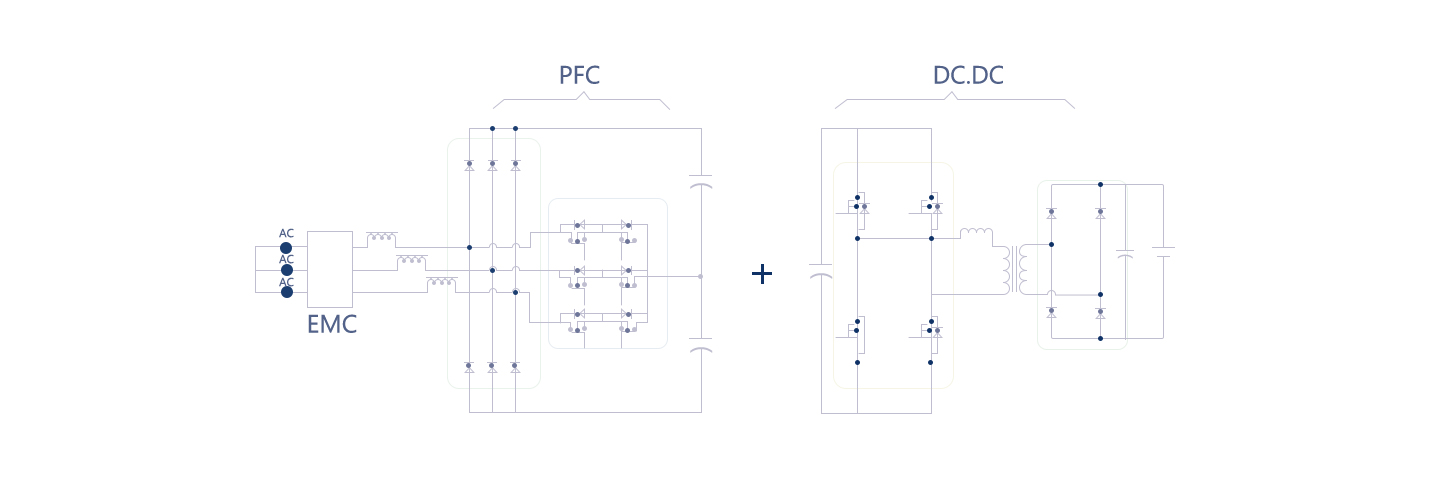
Topdiode SiC Schottky Barrier Diode Used on DC charging pile
With an eye to the goal set by China government, that is, to have 6.543 million electric vehicles running on the roads by 2025, and to increase the ratio of charging piles to electric vehicles to 2.25 by 2025, there will be a huge demand for efficient charging modules and cost-effective charging piles. Meet the huge growth of infrastructure. In high-power and high-temperature environments, silicon carbide devices show obvious advantages over current silicon-based devices in terms of efficiency and cost.
Topdiode Recommended Products:
SiC Diode:TPDD20A120C1P,TPD40A120C1P
SiC Mosfet:TPMW30N120C1P

Topdiode Silicon Carbide (SiC) Schottky Diode Applications



Silicon carbide (SiC), a semiconductor compound consisting of silicon (Si) and carbon (C), belongs to the wide bandgap (WBG) family of materials. Its physical bond is very strong, giving the semiconductor a high mechanical, chemical and thermal stability. The wide band gap and high thermal stability allow SiC devices to be used at junction temperatures higher than those of silicon, even over 200°C. The main advantage offered by silicon carbide in power applications is its low drift region resistance, which is a key factor for high-voltage power devices.
Silicon Carbide Schottky Barrier Diodes are semiconductor devices that consist of a metal contact on a layer of n-type Silicon Carbide (SiC) material. The metal contact forms a Schottky barrier with the SiC material, which allows the flow of current in only one direction. SiC Schottky barrier diodes offer several advantages over conventional diodes, including lower forward voltage drop, shorter reverse recovery time, higher breakdown voltage, and higher temperature operation
The working principle of a Silicon Carbide (SiC) Schottky diode is based on the metal-semiconductor junction known as the Schottky barrier. When a metal (typically aluminum or platinum) is deposited on a SiC substrate, a Schottky barrier is formed between the metal and the semiconductor material. Unlike traditional P-N junction diodes, the Schottky diode does not have a depletion region, which leads to a lower forward voltage drop and faster switching speed.
In forward bias, the metal contact is connected to the positive terminal of a voltage source, while the SiC substrate is connected to the negative terminal. When a positive voltage is applied, the electrons from the metal contact are injected into the SiC substrate, resulting in a flow of current through the device. The forward voltage drop in a SiC Schottky diode is typically lower than in a traditional P-N junction diode, which leads to lower power losses and higher efficiency.
In reverse bias, the metal contact is connected to the negative terminal of a voltage source, while the SiC substrate is connected to the positive terminal. When a negative voltage is applied, the Schottky barrier width increases, and the electric field across the device increases, leading to a breakdown of the device at a certain voltage, known as the reverse breakdown voltage. The reverse breakdown voltage of SiC Schottky diodes is typically higher than in traditional P-N junction diodes, which makes them suitable for high-voltage applications.
- Switching Mode Power Supplies (SMPS)
- AC/DC power supplies
- DC/DC converters
- Industrial power supplies
- Telecom and server power supplies
- Battery chargers
- Inverter and power conversion systems
- Freewheeling diode applications
- High-frequency rectification circuits
Our SiC Schottky Barrier Diodes (SBDs) increase efficiency and add superior reliability in high-voltage applications. SiC diodes exhibit higher breakdown voltage with a lower forward voltage drop and a significantly shorter reverse recover time. SiC SBDs are designed with balanced surge current, forward voltage, thermal resistance and thermal capacitance ratings at low reverse current for lower switching loss, enabling more efficient power systems.