


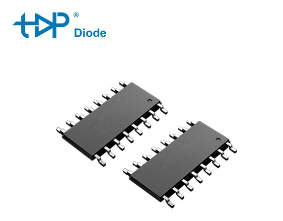
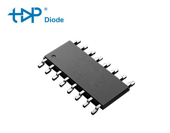
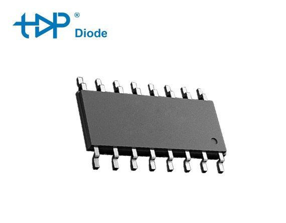
TP3525 Series REGULATING PWM IC Topdiode
* Input Voltage: 8~35V
* On-chip +5.1V reference is trimmed to ±1%
* 100HZ ~ 400KHZ oscillator range
* Separate oscillator sync terminal
* Adjustable dead time control
* Internal soft-start
* Pulse-by-pulse shutdown
* Input under-voltage lockout with hysteresis
* Latching PWM to prevent multiple pulses
* Dual source/sink output drivers
TP3525 Series REGULATING PWM IC Topdiode
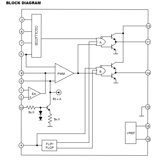
The TP3525 is a pulse width modulator IC and designed for switching power supplies application to improve performance and reduce external parts usage.
A shutdown terminal controls both the soft-start circuitry and the output stages, providing instantaneous turn off through the PWM latch with pulsed shutdown, as well as soft-start recycle with longer shutdown commands. The output stage features NOR logic, giving a LOW output for an OFF state. An under-voltage lockout circuitry, which keeps the outputs off and the soft-start capacitor discharged for sub-normal input voltages, includes approximately 500 mV of hysteresis for jitter free operation. The PWM circuits also feature a latch following the comparator. When a PWM pulses has been terminated, the outputs will remain off for the duration of the period. The latch is reset with each clock pulse. The output stages are totem-pole designs capable of sourcing or sinking in excess of 200mA.
Topdiode TP3525 Series REGULATING PWM IC DATA
- Tab
ABSOLUATE MAXIUM RATINGS
| PARAMETER | SYMBOL | RATINGS | UNIT |
| Supply Voltage | ViN | 40 | V |
| Collector Supply Voltage | VC | 40 | V |
| Oscillator Charging Current | IOSC | 5 | mA |
| Output Current, Source or Sink | Io | 500 | mA |
| Reference Output Current | IR | 50 | mA |
| Current through CT Terminal Logic Inputs Analog Inputs |
IT | 5 – 0.3 ~ + 5.5 -0.3 ~ Vi |
mA V V |
| Total Power Dissipation at Ta=70 °C | PD | 1000 | mW |
| Junction Temperature | TJ | -55 ~ +125 | °C |
| Operating Ambient Temperature | TORP | 0 ~ +70 | °C |
| Storage Temperature | TSTG | -65 ~ +150 | °C |
| Note: Absolute maximum ratings are those values beyond which the device could be permanently damaged. Absolute maximum ratings are stress ratings only and functional device operation is not implied. |
|||
RECOMMENDED OPERATING CONDITIONS (NOTE)
| PARAMETER | SYMBOL | RATINGS | UNIT |
| Input Voltage | VIN | 8 ~ 35 | V |
| Collector Supply Voltage | VC | 4.5 ~ 35 | V |
| Sink/Source Load Current (steady state) | ISTEAD | 0 ~ 100 | mA |
| Sink/Source Load Current (peak) | IPEAK | 0 ~ 400 | mA |
| Reference Load Current | ILOAD | 0 ~ 20 | mA |
| Oscillator Frequency Range | FO | 100 ~ 400K | Hz |
| Oscillator Timing Resistor | RO | 2 ~ 150 | KΩ |
| Oscillator Timing Capacitor | CO | 0.001 ~ 0.1 | μF |
| Dead Time Resistor Range | RT | 0 ~ 500 | Ω |
| Note: Range over which the device is functional and parameter limits are guaranteed. | |||
THERMAL DATA
| PARAMETER | SYMBOL | RATING | UNIT | |
| Thermal Resistance Junction-ambient | DIP16 | θJA | 80 | °C/W |
| SOP-16 SOP-16W TSSOP-16 | θJA | 50 | °C/W | |
| Note: Thermal resistance junction-alumina with the device soldered on the middle of an alumina supporting substrate measuring 15×20 mm; 0.65 mm thickness with infinite heat sink. |
||||
ELECTRICAL CHARACTERISTICS (VIN= 25V, unless otherwise specified)
| PARAMETER | SYMBOL | TEST CONDITIONS | MIN | TYP | MAX | UNIT |
| REFERENCE SECTION | ||||||
| Output Voltage | VREF | TJ= 25°C | 5 | 5.1 | 5.2 | V |
| Total Output Variation (Note 1) | Line, Load and Temperature | 4.95 | 5.25 | V | ||
| Long Term Stability (Note 1) | △VREF | TJ= 125°C, 1000 hrs | 20 | 50 | mV | |
| Line Regulation | △VREF | VIN= 8 ~ 35 V | 10 | 20 | mV | |
| Load Regulation | △VREF | IL = 0 ~ 20 mA | 20 | 50 | mV | |
| Temp. Stability (Note 1) | △VREF/△T | Over Operating Range | 20 | 50 | mV | |
| Output Noise Voltage (Note 1) | 10 Hz ≤ f ≤ 10 kHz, TJ = 25°C | 40 | 200 | μVrms | ||
| Short Circuit Current | VREF = 0, TJ = 25°C | 80 | 100 | mA | ||
| OSCILLATOR SECTION | ||||||
| Clock Amplitude (Note 1, 2) | 3 | 3.5 | V | |||
| Sync Threshold | 1.2 | 2 | 2.8 | V | ||
| Sync Input Current | Sync Voltage = 3.5 V | 1 | 2.5 | mA | ||
| Current Mirror | IRT = 2 mA | 1.7 | 2 | 2.2 | mA | |
| Maximum Frequency | fMAX | RT = 2 KΩ, CT = 0.001μF | 400 | KHz | ||
| Minimum Frequency | fMIN | RT = 150KΩ, CT = 0.1μF | 100 | Hz | ||
| Clock Width (Note 1, 2) | TJ = 25°C | 0.3 | 0.5 | 1 | μs | |
| Initial Accuracy (Note 1, 2) | TJ = 25°C | ±2 | ±6 | % | ||
| Voltage Stability (Note 1, 2) | VIN = 8 ~ 35 V | ±1 | ±2 | % | ||
| Temperature Stability (Note 1) | △f /△T | Over Operating Range | ±3 | ±6 | % | |
| ERROR AMPLIFIER SECTION (VCM = 5.1 V) | ||||||
| Output Low Level | 0.2 | 0.5 | V | |||
| Output High Level | 3.8 | 5.6 | V | |||
| Input Offset Voltage | VOS | 2 | 10 | mV | ||
| Input Bias Current | Ib | 1 | 10 | μA | ||
| Input Offset Current | Ios | 1 | µA | |||
| Comm. Mode Reject. | CMR | VCM = 1.5 ~ 5.2 V | 60 | 75 | dB | |
| Supply Voltage Rejection | PSR | VIN = 8 ~ 35 V | 50 | 60 | dB | |
| DC Open Loop Gain | RL ≥10 MΩ | 60 | 75 | dB | ||
| DC Transconduct. (Note 1, 3) | 30 KΩ ≤RL≤1 MΩ, TJ = 25°C | 1.1 | 1.5 | ms | ||
| Gain Bandwidth Product (Note 1) | Gv = 0 dB, TJ = 25°C | 1 | 2 | MHz | ||
| PWM COMPARATOR | ||||||
| Input Threshold (Note 2) | Zero Duty-cycle | 0.7 | 0.9 | V | ||
| Maximum Duty-cycle | 3.3 | 3.6 | V | |||
| Input Bias Current (Note 1) | 0.05 | 1 | µA | |||
| Minimum Duty-cycle | 0 | % | ||||
| Maximum Duty-cycle (Note 2) | 45 | 49 | % | |||
| SHUTDOWN SECTION | ||||||
| Soft Start Low Level | VSD = 2.5 V | 0.4 | 0.7 | V | ||
| Shutdown Threshold | To outputs, VSS = 5.1 V, TJ = 25°C | 0.6 | 0.8 | 1 | V | |
| Shutdown Input Current | VSD = 2.5 V | 0.4 | 1 | mA | ||
| Soft Start Current | VSD = 0 V, VSS = 0 V | 25 | 50 | 80 | µA | |
| Shutdown Delay (Note 1) | VSD = 2.5 V, TJ = 25°C | 0.2 | 0.5 | μs | ||
ELECTRICAL CHARACTERISTICS (Cont.)
| PARAMETER | SYMBOL | TEST CONDITIONS | MIN | TYP | MAX | UNIT |
| OUTPUT DRIVERS (each output) (VC = 20 V) | ||||||
| Output Low Level | ISINK = 20 mA | 0.2 | 0.4 | V | ||
| ISINK = 100 mA | 1 | 2 | V | |||
| Output High Level | ISOURCE = 20 mA | 18 | 19 | V | ||
| ISOURCE = 100 mA | 17 | 18 | V | |||
| Under-Voltage Lockout | VCOMP and VSS = High | 6 | 7 | 8 | V | |
| Collector Leakage | IC | VC = 35 V | 200 | µA | ||
| Rise Time (Note 1) | tR | CL = 1 nF, TJ = 25°C | 100 | 600 | ns | |
| Fall Time (Note 1) | tF | CL = 1 nF, TJ = 25°C | 50 | 300 | ns | |
| TOTAL STANDBY CURRENT | ||||||
| Supply Current | IS | VIN = 35 V | 14 | 20 | mA | |
Topdiode Hot Selling Products (6)
-
Topdiode Silicon-carbide (SiC) Schottky Barrier Diode, replace Infineon, On Semi, Littelfuse etc.
-
-
-
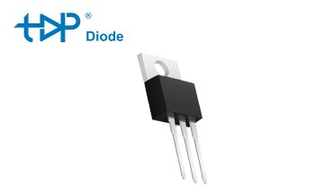
Topdiode Insulated Gate Bipolar Transistors (IGBT), replace Infineon, On semi, ST, AOS etc.
-
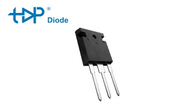
Topdiode Silicon-carbide (SiC) Power MOSFET, replace Infineon, On Semi, ROHM etc.
-
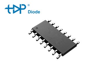
Topdiode Audio Amplifier Audio IC TPA2092 and TPA20957, replace Infineon IRS2092 and IRS20957S
Audio Amplifier IC Datasheet
Topdiode Audio IC Applications



An audio amplifier IC, also known as an integrated circuit, is a small electronic device that amplifies low-power audio signals to a higher power level suitable for driving speakers or headphones.
It combines various components such as transistors, resistors, and capacitors into a single chip, making it compact and efficient. Audio amplifier ICs are commonly used in consumer electronics like smartphones, laptops, televisions, and audio systems to enhance the sound quality and volume output.
It works by taking in an input signal and increasing its amplitude while maintaining the same waveform shape. The basic operation of an audio amplifier IC involves several stages.
First, the input signal is received and passed through a pre-amplification stage where it undergoes initial amplification. This stage helps boost the weak incoming signal to a more usable level.
Next, the amplified signal goes through various processing stages such as filtering and equalization to enhance specific frequency ranges or remove unwanted noise. These stages help improve the overall sound quality before further amplification.
After processing, the signal enters the main amplification stage where it receives significant gain in power. This stage utilizes transistors or other active components within the IC to increase both voltage and current levels of the audio signal.
Finally, once fully amplified, the output from this main stage is sent to drive speakers or headphones directly. The amplified audio signals are then converted back into sound waves by these devices for us to hear. It’s important to note that different types of audio amplifier ICs exist with varying features and capabilities depending on their intended applications (e.g., stereo systems, mobile phones).
However, they all follow similar principles of receiving an input signal, amplifying it at multiple stages while preserving its fidelity and finally delivering high-powered output for listening purposes.
- High power output: It can provide sufficient power to drive speakers and produce loud sound.
- Low distortion: The IC ensures minimal distortion in the amplified audio signal, resulting in high-quality sound reproduction.
- Wide frequency response: It is capable of amplifying a wide range of frequencies, allowing for accurate reproduction of different types of audio signals.
- Small size and compact design: Audio amplifier ICs are often designed to be small and space-efficient, making them suitable for various applications where size is a constraint.
- Efficient power consumption: These ICs are designed to consume less power while delivering optimal performance, making them energy-efficient.
- Built-in protection mechanisms: Many audio amplifier ICs come with built-in protection circuits that safeguard against overvoltage, overheating, short circuits, etc., ensuring the longevity and reliability of the device.
Car amplifiers
Power efficiency – produce sound in speakers, not heat to the surroundings.
Integration – be heard, not seen – smaller and lighter is better, bulky, and heavy is history.
Quality – be robust and flexible, not delicate and demanding.
Cost down – Replacement of Infineon, help our partners cost down