

Topdiode TPP2309 60V P-Channel MOSFET in SOT-23: Cross to Diodes Incorporated ZXMP6A13FTA
The TPP2309 is our 60 V P-channel enhancement mode MOSFET in a SOT-23 package, designed for high-side switches, load switches and battery-path control in space-constrained products. It is pin-to-pin compatible with the Diodes Incorporated ZXMP6A13FTA, with lower guaranteed on-resistance and a faster body diode.
Key Features
- 60 V drain-source voltage and ±20 V gate-source voltage
- RDS(on) max 340 mΩ at -VGS = 10 V; 550 mΩ at 4.5 V
- Low gate charge: 9 nC typ. at 10 V, 4.4 nC typ. at 4.5 V
- Crss 8 pF typ.
- Fast body diode: trr4 ns, Qrr 8 nC (typ.)
- Low leakage: -IDSS max 1 µA at -VDS = 48 V
- Junction temperature range -55 °C to +150 °C
- Compact SOT-23 surface-mount package
Typical Applications
- Battery management: high-side switching, reverse-battery protection, charge/discharge path control
- Portable appliances: load switches, power-path management, power isolation
- DC-DC and power management: high-side switching, level shifting
- General use: adapters, low-power motor drive
Absolute Maximum Ratings (Ta = 25 °C)
| Parameter | Symbol | Value | Unit |
| Drain-source voltage | -VDS | 60 | V |
| Gate-source voltage | VGS | ±20 | V |
| Continuous drain current | -ID | 1.25 | A |
| Pulsed drain current (10 µs pulse width) | -IDM | 8 | A |
| Power dissipation (t ≤ 10 s) | PD | 1.25 | W |
| Operating junction temperature | Tj | -55 to +150 | °C |
| Storage temperature | Tstg | -55 to +150 | °C |
Notes: the 8 A pulsed rating applies to a 10 µs pulse, and the 1.25 W power dissipation applies for t ≤ 10 s. For continuous operation, see Thermal Resistance below.
Thermal Resistance
Junction-to-ambient thermal resistance
| Condition | RθJA max | Power capability at 25 °C ambient |
| t ≤ 10 s | 100 °C/W | 1.25 W |
| Steady state | 166 °C/W | 0.75 W |
Measured on FR-4, 2 oz copper, 1-inch square pad, still air. Power capability = (150 − 25) °C ÷ RθJA. Boards with less copper will have lower capability.
Electrical Characteristics
Static characteristics (Ta = 25 °C)
| Parameter | Symbol | Test condition | Value | Unit |
| Drain-source breakdown voltage | -V(BR)DSS | -ID = 250 µA | ≥ 60 | V |
| Zero-gate-voltage drain current | -IDSS | -VDS = 48 V | ≤ 1 | µA |
| Gate-source leakage | IGSS | VGS = ±20 V | ≤ ±100 | nA |
| Gate threshold voltage | -VGS(th) | VDS = VGS, -ID = 250 µA | 1 to 3 | V |
| Drain-source on-resistance | RDS(on) | -VGS = 10 V, -ID = 1.25 A | ≤ 340 | mΩ |
| Drain-source on-resistance | RDS(on) | -VGS = 4.5 V, -ID = 1 A | ≤ 550 | mΩ |
Drive the gate with at least 4.5 V (10 V for lowest loss). RDS(on) is not specified at 3.3 V and rises steeply below about 4 V (Fig. 3).
Dynamic characteristics (typical, Ta = 25 °C)
| Parameter | Symbol | Test condition | Typ. | Unit |
| Input capacitance | Ciss | -VDS = 30 V, VGS = 0 V, f = 1 MHz | 589 | pF |
| Output capacitance | Coss | As above | 35 | pF |
| Reverse transfer capacitance | Crss | As above | 8 | pF |
| Gate resistance | Rg | VDS = 0 V, VGS = 0 V, f = 1 MHz | 18 | Ω |
| Forward transconductance | gfs | -VDS = 5 V, -ID = 1.25 A | 3.7 | S |
| Total gate charge | Qg | -VDS = 20 V, -VGS = 10 V, -ID = 1.25 A | 9 | nC |
| Total gate charge | Qg | -VDS = 20 V, -VGS = 4.5 V, -ID = 1.25 A | 4.4 | nC |
| Gate-source charge | Qgs | -VDS = 20 V, -VGS = 10 V, -ID = 1.25 A | 2 | nC |
| Gate-drain charge | Qgd | As above | 1.3 | nC |
| Turn-on delay time | td(on) | -VGS = 10 V, -VDS = 15 V, -ID = 1 A, RG = 24 Ω | 18 | ns |
| Turn-on rise time | tr | As above | 14 | ns |
| Turn-off delay time | td(off) | As above | 28 | ns |
| Turn-off fall time | tf | As above | 7 | ns |
Gate-drive loss (Qg × -VGS × f) at 100 kHz is about 9 mW at 10 V and 2 mW at 4.5 V.
Body diode (Ta = 25 °C)
| Parameter | Symbol | Test condition | Value | Unit |
| Body diode voltage | -VSD | -IS = 1.25 A, VGS = 0 V | ≤ 1.2 | V |
| Continuous current | -IS | Continuous | ≤ 1.25 | A |
| Reverse recovery time | trr | -IS = 1.25 A, di/dt = 100 A/µs | 12.4 typ. | ns |
| Reverse recovery charge | Qrr | As above | 8 typ. | nC |
If the body diode must carry current continuously, loss can reach 1.5 W at 1.25 A (1.2 V × 1.25 A), above the steady-state power budget. Turn the channel on during conduction instead.
Package, Marking and Packing
| Item | Detail |
| Package | SOT-23 |
| Pin assignment | 1 = gate, 2 = source, 3 = drain |
| Marking | M29, followed by YM year/month code |
| Recommended footprint | 0.8 × 1.0 mm pads, 1.9 mm pitch between the two lower pads, 2.0 mm overall |
| Tape width / pitch | 8 mm / 4 ± 0.1 mm |
| Reel | 7 in (178 mm), 3,000 pcs |
The drain pad (pin 3) is the heatsink. Add copper on the drain net and thermal vias where possible.
TPP2309 vs. ZXMP6A13FTA
Parameter Comparison
| Parameter | TPP2309 | ZXMP6A13FTA |
| Package / pin-out (1 / 2 / 3) | SOT-23, G / S / D | SOT23, G / S / D |
| -V(BR)DSS min | 60 V | 60 V |
| -VGS(th) | 1 to 3 V | 1 to 3 V |
| RDS(on) max, -VGS = 10 V | 340 mΩ @ 1.25 A | 400 mΩ @ 0.9 A |
| RDS(on) max, -VGS = 4.5 V | 550 mΩ @ 1 A | 600 mΩ @ 0.8 A |
| Continuous -ID | 1.25 A (board not stated) | 1.1 A (TA = 25 °C, 25 × 25 mm FR4) |
| Ciss typ. (-VDS = 30 V, 1 MHz) | 589 pF | 219 pF |
| Crss typ. (-VDS = 30 V, 1 MHz) | 8 pF | 20.5 pF |
| Qg typ., -VGS = 10 V | 9 nC (-VDS = 20 V, -ID = 1.25 A) | 5.9 nC (-VDS = 30 V, -ID = 0.9 A) |
| Body diode trr / Qrr typ. | 12.4 ns / 8 nC (1.25 A) | 21.1 ns / 19.3 nC (0.9 A) |
Competitor figures: Diodes Incorporated ZXMP6A13F datasheet, DS32014 Rev. 7-2, November 2013.
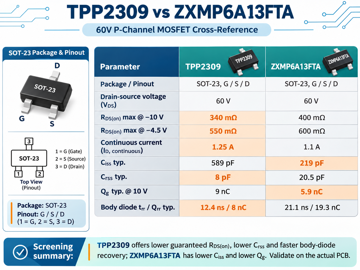
The TPP2309 offers lower guaranteed RDS(on) (340 vs. 400 mΩ at 10 V, about 15% lower; 550 vs. 600 mΩ at 4.5 V, about 8% lower), lower Crss (8 vs. 20.5 pF) and a faster body diode (trr 12.4 vs. 21.1 ns; Qrr 8 vs. 19.3 nC). The ZXMP6A13FTA has lower input capacitance (219 vs. 589 pF) and lower gate charge (5.9 vs. 9 nC at 10 V).
Some rows are not like-for-like. The continuous-current ratings (1.25 A vs. 1.1 A) are not measured on the same board, so they are not a like-for-like current advantage, and the gate-charge figures use different drain voltages. The competitor marks its capacitance and recovery figures as design aid only. Compare the two on your own board.
Design-in Checklist
- Keep worst-case voltage, including transients, under 60 V; a working voltage near 48 V leaves margin.
- Drive the gate with at least 4.5 V, and 10 V for lowest loss. Do not rely on 3.3 V logic.
- Calculate conduction loss at your hottest junction temperature, using about 1.8× RDS(on) at 150 °C (Fig. 4).
- Budget about 0.75 W at 25 °C ambient for continuous operation, and less when the board is warm.
- Avoid sustained body-diode conduction.
- The 8 A rating is for a 10 µs pulse. No SOA curve is published, so validate repetitive or inductive pulses on your board.
- Add copper under the drain pad; the datasheet figures assume a 1-inch square pad.
FAQ
Is the TPP2309 a drop-in replacement for the ZXMP6A13FTA?
Package and pin-out match (pin 1 gate, pin 2 source, pin 3 drain), and both parts share the 60 V rating, ±20 V gate rating and 1 to 3 V threshold range. The TPP2309 has lower guaranteed RDS(on), but its typical input capacitance (589 pF) and gate charge (9 nC at 10 V) are higher than the ZXMP6A13FTA’s (219 pF, 5.9 nC), measured under different conditions. Check the gate driver and edge rates in fast-switching designs, then validate on your board.
Can I drive it directly from a 3.3 V microcontroller pin?
Not reliably. The threshold can reach 3 V and RDS(on) is only specified at 4.5 V and 10 V. Use a level shifter or gate driver.
Does the 1.25 A rating hold continuously?
On the reference board it corresponds to the short-duration (t ≤ 10 s) rating. For continuous operation, use the 0.75 W steady-state budget in Table 2 as a starting point and verify thermally in your design.
Can two devices be paralleled for more current?
Yes, with symmetric layout and individual gate resistors, but RDS(on) rises with temperature, which helps current sharing. Validate with thermal imaging on the actual board.
Does it work for reverse-battery protection?
Yes, as a high-side P-channel in series with the load, with the gate referenced to ground through a resistor. Keep VGS within ±20 V; add a zener clamp if the supply can exceed that.
Contact: www.topdiode.com | zoe@topdiode.com